Understanding Zero PCB: A Comprehensive Guide to Prototyping, Design, and Applications
Printed Circuit Boards (PCBs) are the backbone of all modern electronics, enabling complex circuits to be compact, efficient, and reliable. But before mass production begins, engineers and hobbyists often need a quick and flexible way to test circuits — this is where Zero PCB comes in. Zero PCB is one of the most essential tools for electronics prototyping, allowing designers to assemble and test circuits without the need for full PCB fabrication.
In this guide, we’ll explore everything about Zero PCB — what it is, how it works, its advantages, limitations, and how manufacturers like globalwellpcba.com can help you move from a Zero PCB prototype to a professional, production-ready PCB.
What is a Zero PCB?
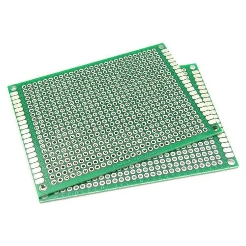
A Zero PCB (also known as a general-purpose PCB or universal PCB) is a type of board used primarily for prototyping and testing electronic circuits. Unlike traditional printed circuit boards, which are custom-made with designed copper tracks, a Zero PCB comes pre-drilled with holes arranged in a grid pattern and often includes individual copper pads or strip connections.
This allows engineers, students, and hobbyists to manually connect components using solder or jumper wires, giving them flexibility to modify the circuit design during experimentation.
Common Names
Zero PCBs are known by various names, including:
- General-purpose PCB
- Perforated board
- Universal board
- Protoboard
- Veroboard (in strip form)
Despite these variations, the purpose remains the same — to test and verify circuit functionality before final PCB fabrication.
Structure and Design of Zero PCB
Zero PCBs come in various designs and materials. Understanding their structure helps in choosing the right type for your project.
Board Material
The most common materials include:
- FR-1 or FR-2: Made of phenolic resin; inexpensive and suitable for low-stress projects.
- FR-4: Made from glass-reinforced epoxy laminate; more durable and suitable for permanent prototypes.
Hole Grid
Typically, the holes on a Zero PCB are spaced 0.1 inch (2.54 mm) apart, matching the pin spacing of through-hole components like resistors, capacitors, transistors, and ICs.
Copper Pads
There are two main types of copper patterns:
- Individual Pads: Each hole is surrounded by a separate copper ring, allowing full design flexibility.
- Striped Pads: Holes are connected in rows (similar to veroboards), simplifying straight connections but limiting flexibility.
Sizes
Zero PCBs come in multiple standard sizes, such as:
- 5 cm x 7 cm
- 7 cm x 9 cm
- 10 cm x 15 cm
- 12 cm x 18 cm
The choice depends on the circuit’s complexity and component count.
The Purpose of Using Zero PCB
Zero PCBs are invaluable in early design and experimentation phases. Here’s why they’re widely used:
- Prototyping: Quickly test and modify circuit designs.
- Education: Ideal for students learning circuit assembly and soldering.
- Debugging: Helps in analyzing performance before PCB manufacturing.
- Temporary Builds: Useful for short-term projects where custom PCBs are unnecessary.
- Component Testing: Engineers can test ICs, transistors, and new components.
Zero PCB allows freedom to experiment, something not always possible with prefabricated boards.
Advantages of Using Zero PCB
Cost-Effective
Since Zero PCBs are inexpensive and reusable, they are perfect for budget-friendly prototyping.
Flexibility
You can create any circuit layout manually, connect components as needed, and easily modify them later.
Readily Available
They are available in almost all electronics stores and online platforms, making them accessible worldwide.
Great for Learning
Beginners can gain hands-on experience with soldering, wiring, and debugging.
No Fabrication Delay
Unlike custom PCBs that take days to fabricate, Zero PCB allows instant circuit building.
Limitations of Zero PCB
While versatile, Zero PCBs also come with several challenges:
- Time-Consuming: Manual wiring and soldering take longer.
- Messy Layouts: As the circuit grows, wires may become tangled and confusing.
- Error-Prone: Manual soldering increases the chance of mistakes.
- Limited Reliability: Connections may loosen or degrade over time.
- No High-Frequency Support: Zero PCBs aren’t suitable for high-frequency or precision circuits.
For final products or industrial projects, moving from Zero PCB to a professional PCB from manufacturers like globalwellpcba.com is recommended.
Types of Zero PCBs
Zero PCBs are available in various configurations depending on your project type.
Single-Sided Zero PCB
Copper pads exist on only one side — simple and affordable, best for small circuits.
Double-Sided Zero PCB
Copper pads on both sides allow denser and more complex circuit designs.
Pre-Striped Zero PCB
Rows of connected pads simplify the creation of buses or IC sockets.
SMD-Compatible Zero PCB
Special Zero PCBs support Surface Mount Devices (SMD), featuring smaller pad spacing.
Gold-Plated Zero PCB
These use ENIG (Electroless Nickel Immersion Gold) plating for better conductivity and corrosion resistance, suitable for long-term use.
How to Use Zero PCB: Step-by-Step Guide
Let’s go through the practical steps to use a Zero PCB for building a circuit.
Design Your Circuit
Draw your circuit on paper or using software (like KiCAD or Fritzing). Identify component placement before soldering.
Gather Components
Collect resistors, capacitors, ICs, wires, and connectors. Ensure they are through-hole components unless using SMD Zero PCBs.
Place Components
Insert components into the holes as per the schematic. Leave enough space for easy soldering.
Solder Connections
Solder each component lead to the copper pad. Use a clean soldering iron tip and quality solder wire for strong joints.
Make Electrical Connections
Use:
- Jumper wires for cross-connections.
- Copper wires for long paths.
- Solder bridges for short connections.
Test the Circuit
Check continuity with a multimeter before powering the circuit. Once tested, apply power and observe behavior.
Modify if Necessary
If something doesn’t work, desolder and rewire. That’s the beauty of Zero PCB — you can easily modify designs.
Applications of Zero PCB
Zero PCBs are used in a wide range of educational, commercial, and research applications.
Educational Projects
In schools and universities, Zero PCBs are perfect for electronics labs where students build:
- LED blinkers
- Amplifiers
- Power supplies
- Sensor modules
Research & Development
Engineers and startups use Zero PCBs to rapidly prototype and test new product concepts.
Hobby Electronics
Makers and DIY enthusiasts build:
- Robots
- IoT devices
- Home automation circuits
Repair & Testing
Technicians use Zero PCB to test new component configurations or create custom adapters.
Pre-Production Prototyping
Before mass production, prototypes are often assembled on Zero PCBs for functional testing.
From Zero PCB to Professional PCB
Once the prototype works, it’s time to move to a custom-designed PCB for durability and mass production. Manufacturers like globalwellpcba.com provide full PCB fabrication and assembly services — taking your tested Zero PCB design to the next level.
Why Transition from Zero PCB?
- Improved reliability and signal integrity
- Reduced noise and interference
- Compact, repeatable layouts
- Suitable for automated assembly
- Professional appearance for commercial use
How globalwellpcba.com Helps
Global Well PCBA specializes in:
- PCB Design and Layout
- Multilayer PCB Fabrication
- Component Sourcing
- SMT & Through-Hole Assembly
- Quality Testing & Inspection
With their expertise, you can transform your prototype from a messy Zero PCB into a fully functional, production-grade electronic product.
Zero PCB vs Breadboard vs Custom PCB
| Feature | Zero PCB | Breadboard | Custom PCB |
|---|---|---|---|
| Reusability | Limited | High | None |
| Soldering Required | Yes | No | Yes (machine/hand) |
| Durability | High | Low | Very High |
| Cost | Low | Medium | Medium to High |
| Time to Build | Moderate | Fast | Slow |
| Ideal For | Semi-permanent prototypes | Quick experiments | Final product |
Breadboards are great for initial testing, Zero PCBs for stable prototypes, and custom PCBs for final products.
Tips for Working with Zero PCB
To make the most of your Zero PCB projects, consider these practical tips:
- Plan Layout: Sketch the design to avoid crossing wires unnecessarily.
- Use Color Codes: Color-code wires for power, ground, and signal.
- Label Components: Mark ICs and connections to simplify debugging.
- Avoid Overheating Pads: Excessive soldering heat can lift copper pads.
- Keep Wires Short: Reduces resistance and improves reliability.
- Use Heat Shrink Tubing: For insulation and neat appearance.
- Test Frequently: After adding each section, test continuity and function.
- Document the Design: Helps in replicating or troubleshooting later.
Future of Prototyping: Combining Zero PCB and Rapid PCB Manufacturing
As electronics design evolves, hybrid prototyping — combining Zero PCB experimentation with rapid PCB fabrication — is becoming a trend. Services like globalwellpcba.com offer quick-turn PCB manufacturing, allowing designers to order small batches of custom boards in just days.
This bridges the gap between manual prototyping and mass production, making development cycles faster and more efficient.
Common Mistakes When Using Zero PCB
Even experienced users make errors during prototyping. Here are the most common ones to avoid:
- Incorrect Power Polarity: Can damage components instantly.
- Overlapping Wires: Causes accidental short circuits.
- Cold Solder Joints: Lead to intermittent connections.
- Lack of Ground Plane: May result in noisy signals.
- Improper Heat Dissipation: Especially for high-current circuits.
- No Documentation: Makes debugging nearly impossible.
Preventing these mistakes saves time and ensures a smooth transition to a final PCB design.
Environmental Considerations
Soldering on Zero PCB involves lead-based solder and plastic insulation, which must be handled responsibly.
- Use lead-free solder whenever possible.
- Dispose of waste components and solder residues properly.
- Reuse Zero PCBs by desoldering components carefully.
Manufacturers like Global Well PCBA also follow RoHS (Restriction of Hazardous Substances) compliance to ensure eco-friendly PCB production.
Why Choose Global Well PCBA for Your PCB Projects
If you’ve completed your Zero PCB prototype and are ready for professional fabrication, globalwellpcba.com is the ideal next step. Here’s why:
Expertise
With years of experience in PCB manufacturing and assembly, Global Well PCBA provides advanced solutions tailored to your project.
High Precision
They offer rigid, flex, and Rigid-Flex PCBs with micro-vias, impedance control, and high-frequency capabilities.
Full-Service Support
From design optimization to component procurement, everything is handled under one roof.
Rapid Turnaround
Their quick-turn services mean you can receive prototype boards within days — ideal for fast-moving R&D environments.
Global Reach
No matter where you are, you can order directly from globalwellpcba.com, ensuring smooth logistics and communication.
Conclusion: The Role of Zero PCB in Modern Electronics Development
Zero PCB remains one of the most valuable tools in the toolkit of engineers, educators, and electronics enthusiasts. It provides an affordable, flexible, and practical way to bring circuit ideas to life. Though it’s not suitable for final production, it plays a critical role in rapid prototyping, experimentation, and circuit validation.
As technology advances, the journey from a simple Zero PCB prototype to a high-performance PCB has become easier than ever — thanks to expert manufacturers like globalwellpcba.com who bridge the gap between concept and creation.